
Singapore Polytechnic - Digital Electronics Stop Watch
Link to github: Github link
Introduction
‘Digital Electronics 1’ introduces students to the knowledge, understanding and design techniques necessary to enable them to design simple combinational circuits using commercial SSI and MSI integrated circuits. Additional topics covered include introduction to simple sequential logic circuits such as flipflops and mono-stables.
‘Digital Electronics 2’ builds on basic material covered earlier with advanced topics such as adders, multiplexers/ demultiplexers, decoders/ encoders, counters and shift registers and some application examples of these circuits.
Note The project in ‘Digital Electronics 1’ is done purely in simulation. Hence this post will only focus on the project created in ‘Digital Electronics 2’.
Task
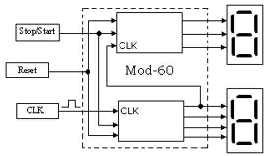
Students were tasked with designing and constructing a 60-second stop watch with start/stop and reset functions.
Requirements
- A counter that count in the decimal numeric sequence from 00 to 59 before resetting to 00.
- A ‘Reset’ push button that resets the counter to 00 when activated. The counter will then remain at 00 until it is started again through the use of the Start/Stop switch
- A ‘Start’ and ‘Stop’ switch that starts stop the counter at its current count value respectively.
 |
| Figure of counter |
Video demonstration
Solution
The following segments documents the actions used to fulfill the requirements
Circuit board design
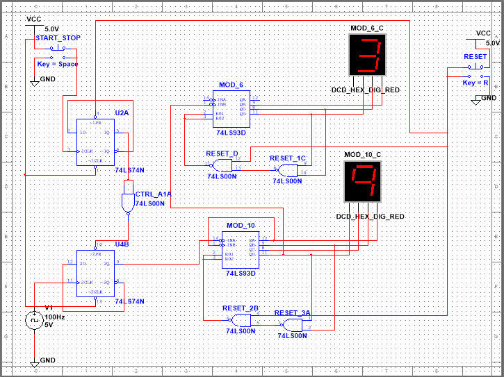 |
| Multi-sim design |
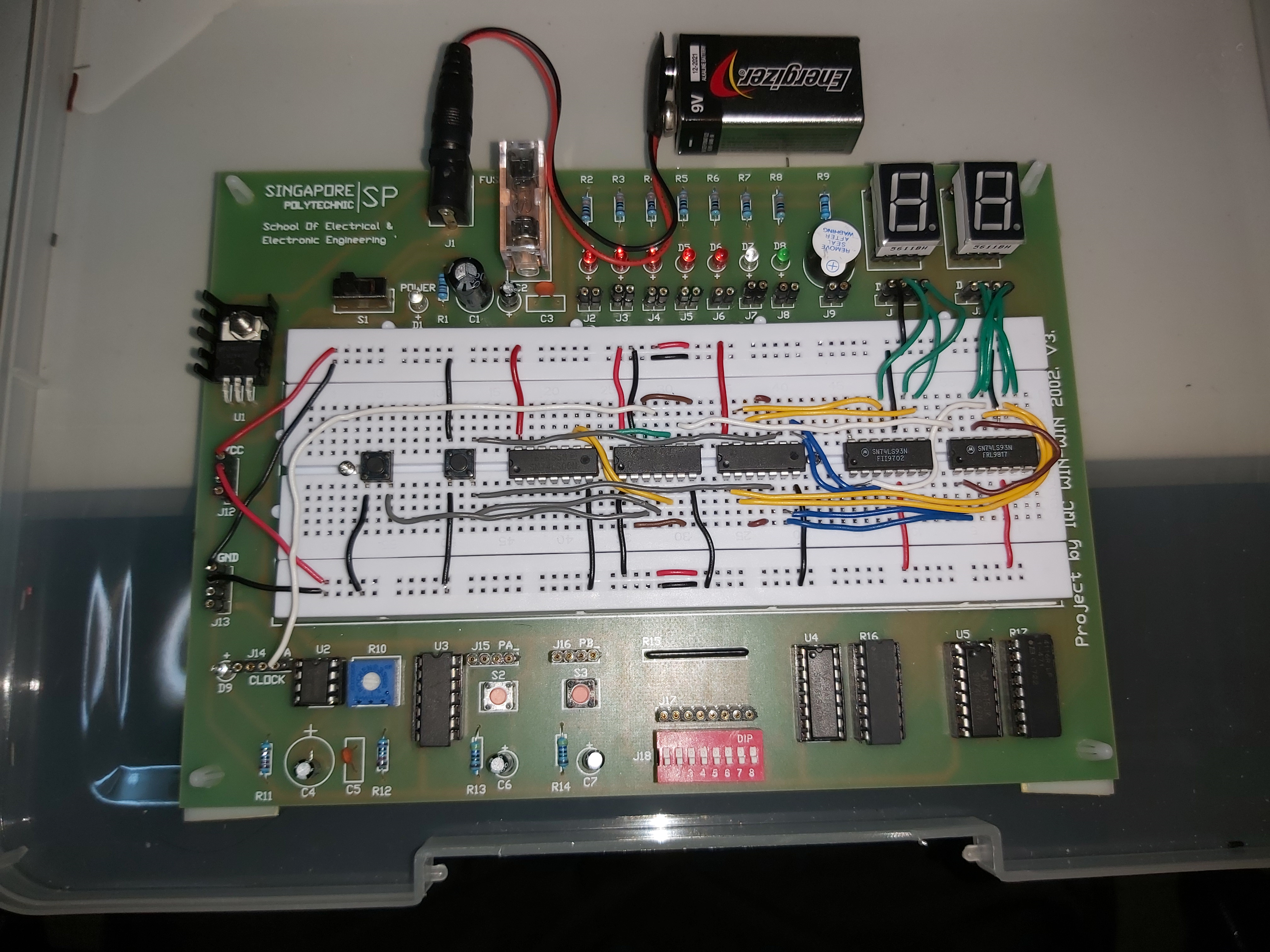 |
| Circuit board design |
MOD 60 logic MOD 60= MOD 6 * MOD 10 Bin:10=1010 Bin:6=0110 Therefore, to achieve MOD 10, reset needs to be connected to Q:B and Q:D. Similarly, to achieve MOD 6, reset needs to be connected to Q:B and Q:C.
Reset logic
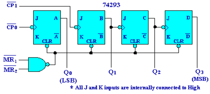 |
| Internal layout of a 74LS293 |
From the Internal layout of a 74LS293 and Multi-sim diagrams, we can see that the reset logic is as follows:
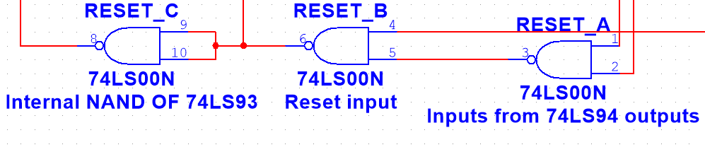 |
| Reset logic |
Using boolean algebra, 2 NAND gate equals 1 AND gate.
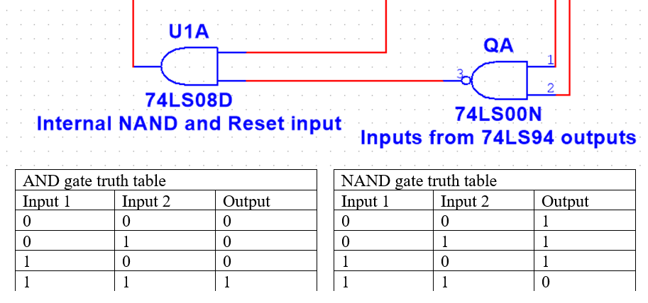 |
| 2 NAND gate = 1 AND gate |
The RESET switch outputs Logic: High by default. The output of the NAND gates is also Logic: High until both inputs are Logic: High.
Therefore, the only times that AND gate output will be Logic: Low is either when the RESET switch is triggered or when the respective MODs reach their reset points. This allows effective resetting of the MOD 60 counter as the CLR inputs are level-trigger logic low.
Start-Stop logic Pins 1 to 6 of the 74LS74 will be referred to as Group: A, while pins 8 to 13 will be referred to as Group: B.
Before the Start_Stop button is pressed. Pin 5 is connected to a NAND gate, whose output is connected to pin 10 of Group: B. This ensures a Logic: High output at pin 9, which is connected to the CLK input of MOD 10 counter. This prevents the counter from starting the count without user input.
When the Start_Stop button is pressed, the output of Group: A toggles. This causes the output of the NAND gate to become Logic: High. This effectively disables the asynchronous functions of Group: B, allowing the clock signal to be applied, hence beginning the count.
All CLR inputs are connected to Logic: High to remove them from the equation. The RESET switch is connected to the PRE input of Group: A. The RESET switch has a default of Logic: High, allowing for synchronous operations. When the RESET switch is pressed, the output of Group: A will be toggled, thus toggling the output of the NAND gates, and overwriting the output of Group: B. This allows the RESET switch to both reset the circuit and pause the MOD 60 counter.
Reflections
I have learnt the following through this project: Firstly, I have learned the importance of building the circuit instead of relying on Multi-sim. The constructed board makes trouble shooting overall design of the circuit much easier as it allows me to physically verify each connection. This method was what allowed me to detect an error in multi-sim, which had not been working up to that point, as I did not realize that I was missing 2 crucial connections. Next, I have also learned to factor in defective components while trouble shooting. I initially struggled with the project as I did not realize that one of my IC chips was defective and was giving me erroneous results. I had another issue as both push-buttons on the board were resetting the MOD counters to zero, even if no wires were connected to them. I overcame the defective IC chip by using another IC and worked around the push-buttons by using my own buttons. Lastly, I have learned that re-attaching broken IC pins, while doable, is not recommended as the re-attached pin break off very easily.
The following improvements could have been made: Firstly, cable management could be improved. Most of the cables are twisted and not straight. This makes the circuit look untidy. Secondly, IC placement could be improved. The Reset segment and Start/Stop segment are independent of each other. Therefore, the 74LS93 used control the MOD counter should have been placed between the Rest and Start/Stop segments to make the circuit neater.